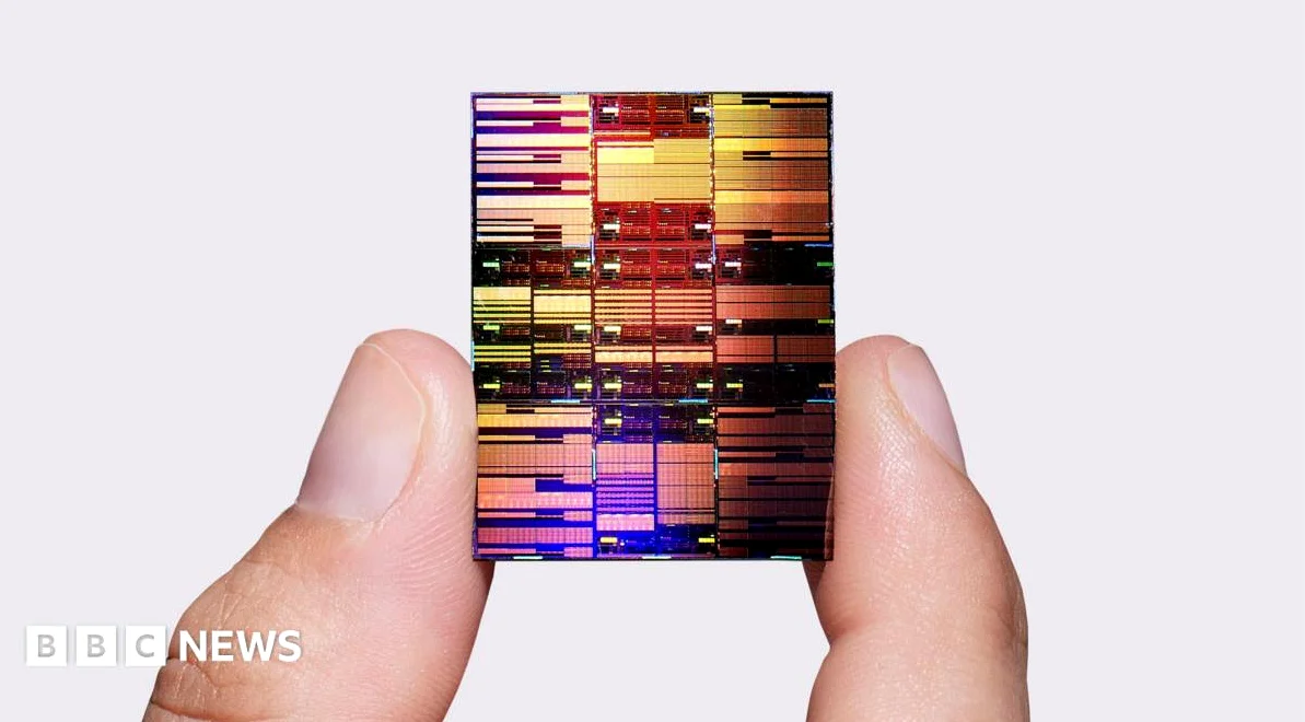
IBM has revealed a new chip design which it says could enable manufacturers to cram 100 billion transistors on a silicon chip the size of a fingernail, according to the BBC.
A New Era in Chip Technology
The current industry-standard size for chips, measured in nanometres—a billionth of a metre and the size of a few atoms—is around two nanometres (nm).
However, IBM claims its new chip tech is the equivalent of around 0.7nm, which may make it the world’s first known chip technology below 1nm.
Despite this breakthrough, it will be several years before the chip tech could be ready to go into production.
In tests, IBM’s prototype performed 50% better than its own 2nm chip and was 70% more energy efficient.
The company reported similar boosts in performance when it debuted its 2nm chip tech back in 2021, stating that tests of those chips produced similar leaps in performance and energy efficiency.
Reinventing Chip Architecture
Jay Gambetta, director of IBM Research and IBM Fellow, described the NanoStack tech as a “landmark moment” for the future of chips.
“With our new NanoStack architecture, we’re not just making smaller transistors, we’re reinventing how chips are built to deliver dramatically more power and energy efficiency,” he said.
Transistor Power and Moore’s Law
Transistors are the building blocks of silicon chips, providing computing power for the world’s electronics, including smartphones, games consoles, and laptops.
They have also become major to the powerful computers housed in data centres, processing a range of everyday digital activities from streaming to online banking and powering the generative AI boom.
The more transistors manufacturers can squeeze onto a chip, the more powerful the chip becomes, and therefore the more devices can do.
For decades, the number of transistors that can be put onto a chip has doubled every two years: this is a phenomenon known as Moore’s Law.
But with billions of transistors now on some chips, it is growing more difficult to sustain this pace, and experts broadly agree this growth cannot continue indefinitely.
In order to try to extend it, rather than try to cram more transistors onto the surface horizontally, chip designers have for some time focused on 3D alternatives, essentially altering the shape of the transistors to make them taller.
IBM’s approach is to layer sheets of them on top of each other as well.
Professor Alan Woodward, a computer scientist at Surrey University, compared it with building a big block of flats rather than houses in a city.
“IBM’s NanoStack is like proposing a 100-storey skyscraper,” he said, adding that in his view, the firm’s closest rivals such as Samsung and Intel are closer to 30-50 storey buildings with their own 3D chip work.
The challenges facing 3D chip designers include heat: the transistors can get hot as they work and heat rises.
Also, when the layers between them are too thin, sometimes this prevents them from switching off when they’re supposed to, and this stops the chip from working.
“I think it’s fair to say IBM’s proposals are the most ambitious,” said Prof Woodward.


Comments
No comments yet
Be the first to share your thoughts